|
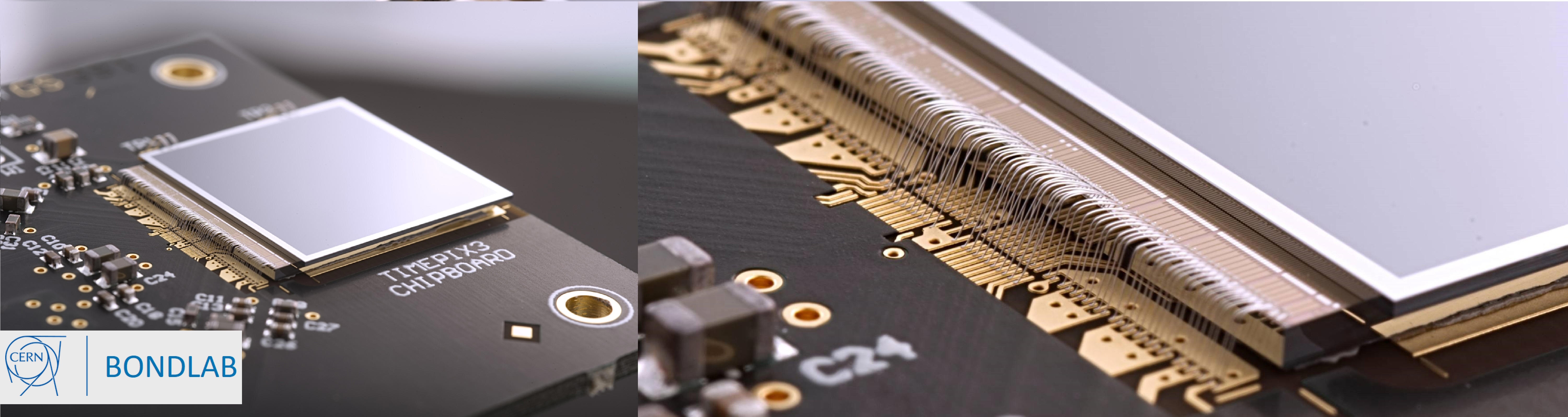
What is wirebonding?
Wirebonding is an electrical interconnect technology developed by
microelectronics industry and today used excessively in (solid state) detector
construction. It allows to interconnect electronic chips, printed circuit
boards, pitch adapters and solid state sensors.
The Wirebonding technique is
a solid phase welding process which uses thin wire and a combination of heat,
pressure and/or ultrasonic energy.
What
types of wirebonding processes exist?
Wirebonding process begins
by firmly attaching the backside of a chip to a chip carrier using either an
organic conductive adhesive or a solder
(Die
Attach).
The wires then are welded
using a special bonding tool (capillary or wedge).
Depending on bonding agent,
we can identify three major wirebonding processes:
|
Wirebonding processes
|
Pressure
|
Temperature
|
Ultrasonic energy
|
Wire
|
Pad
|
|
Thermocompression
|
High
|
300-500 oC
|
No
|
Au,
|
Al, Au
|
|
Ultrasonic
|
Low
|
25 oC
|
Yes
|
Au, Al
|
Al, Au
|
|
Thermosonic
|
Low
|
100-150 oC
|
Yes
|
Au
|
Al, Au
|
Alternatives
to wire bonding
Tape Automated Bonding (TAB)
uses thin Cu beams instead of wires. The beams are held in place by thin polymer
tapes (usually Polyimide) and form a microcable.
The STAR experiment (BNL)
and ALICE are employing a form of TAB technology.
Flip chip bonding, often also referred to as bump bonding
currently provides the highest connection density. Invented in the mid 1960s,
the technology uses bumps (conductive polymers, Indium or solder bumps,
microballs) instead of wired to bond the flipped chip to a substrate. In HEP the
flip chip technology is so far exclusively used in the construction of Si pixel
detectors, where a Si sensor, segmented as area array of individual diodes need
to be connected to the readout chip, correspondingly segmented.
The
Bondlab is performing exclusively Ultrasonic Wedge Bonding with Aluminum wire.
|